Evaluate Flatness
Since first being produced in the 1960’s, silicon wafer technology has progressed at an incredible rate. Today’s wafers must be free of defects to be of any use – standard wafers are now less then 300μm thick and shrinking. In addition, many components are now just a few nanometres in size, which means even a microscopic defect could render an entire device useless.
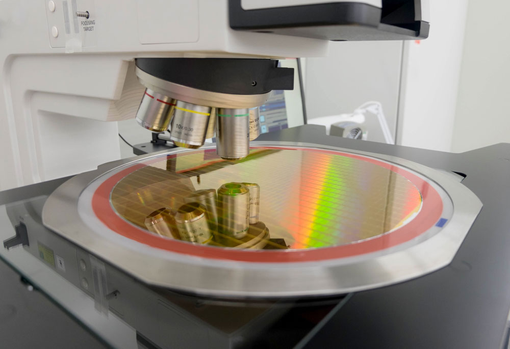
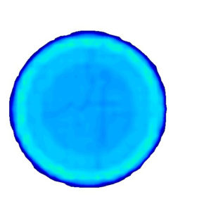
Modern silicon wafer processing techniques must be excruciatingly precise. In particular, wafer grinding equipment used to thin and polish silicon wafers must apply uniform pressure. Pressure profiles of polishing heads can be evaluated using XSENSOR’s high accuracy, high resolution LX sensors. This is especially important in wafer polishing applications where equipment is designed to remove microns at a time.
XSENSOR’s LX pressure sensors maintain calibration and accuracy during repeated testing, ensuring you can accurately compare pressure profiles taken before and after adjustments are made. Adjustments can also be made while viewing pressures in real time.
Specifications & Performance:
| SENSOR | SENSEL SIZE (mm) | SENSING AREA (cm x cm) | CALIBRATION RANGE N/cm2 (psi) | RESOLUTION |
|---|---|---|---|---|
| LX100:100.100.10 | 2.54 | 25.4 x 25.4 | 0.07-2.7 (0.1-3.87) | High |
| LX205:100.100.10 | 2.54 | 25.4 x 25.4 | 0.14-10.34 (.2-15) | High |
Superior Imaging Software for image comparison
XSENSOR Pro software has been the industry leader for interface pressure testing and measurement for many years. Easy-to-use and very stable, Pro V8 provides a feature rich toolkit for image comparison and comprehensive pressure data analysis. The software allows the user a range of options to view 2D and 3D pressure data. Frame and multi-frame compare options provide an easy way to review test stages. Graphing tools are available for review of pressure distribution and pressure over time data. You can select specific frames of data and areas within the image for more detailed analysis.
Pressure Range: 0.14-2.7 N/cm2
We are an ISO 17025 certified pressure imaging sensor manufacturer
Unlike other sensors on the market, our sensors maintain their calibration due to the capacitive technology design used and the unique materials used to make these sensors. Our ISO 17025 accreditation means that we have demonstrated competency in producing accurate test and calibration data from our sensors. Your ISO registration requires your suppliers provide verified calibrated test equipment and recalibration processes to maintain your compliance.